
III. Combinational Logic Design

Word Table
- 组合逻辑(combinational logic)
- 理由(justification)
Design Concepts and Automation
Logic Representation
- 真值表
- 布尔函数
- 卡诺图
- 时序图(timing diagram)
- 逻辑电路图(logic circuit)
Design Procedure
- 系统描述(specification): 指定所需的行为。
- 形式化(formalization):以布尔方程或真值表的方式对系统的输入输出关系进行形式化
- 优化(optimization):优化逻辑的表示,减少成本。
- 工艺映射(technology mapping):将优化后的逻辑设计工艺映射到可以实现的工艺上。
- 验证(verification):验证设计的正确性。
芯片定制(chip design)
- 全定制设计(full customized): 价格贵,性能高,密度高,适合大规模生产。the entire design of the chip down to the details of the layout is finished
- Expensive
- Justifiable only for dense, fast chips with high sales volume
- 标准单元设计(standard cell design): blocks have been designed ahead of time or as part of previous designs
- Intermediate cost
- Less density and speed compared to full customized
- 门阵列设计(gate array design): 密度低,性能低,价格便宜。regular patterns of gate and transistors that can be used in many designs built into chip - only the interconnections between gates are specific to a design
- Lowest cost
- Less 密度(density) compared to full customized and standard cell
Hierarchical Design
对于复杂的数字系统,一种典型的设计方法为分层设计(hierarchical design),即将复杂问题模块化分解为若干层次,然后逐个抽象解决。
- 最小层的模块(block) 叫做原子模块(primitive block)。Any block that cannot be further decomposed is called a primitive block.
- 由不同层级的基本块组成的集合叫做层次结构(hierarchy)。The collection of all blocks including the decomposed ones is a hierarchy.
例:Hierarchy for 9-Input Parity Checker
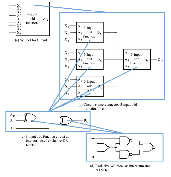
分层设计的设计方法可以分为
- 自顶向下的设计(top-down design):分解功能设计。A top-down design proceeds from an abstract, high-level specification to a more and more detailed design by decomposition and successive refinement. Top-down design answers: What are we building?
- 自底向上的设计(bottom-up design):根据现有的元件去组合成目标功能。A bottom-up design starts with detailed primitive blocks and combines them into larger and more complex functional blocks. Bottom-up design answers: How do we build it?
一般从两个方向同时进行设计。一般 top-down 设计控制复杂度,bottom-up 设计聚焦于细节。
Technology Mapping
工艺映射是指将优化后的逻辑设计工艺映射到有限的工艺上。
比如:因为 NAND 门和 NOR 门是通用门(universal gate),我们可以将任意逻辑电路映射到仅使用 NAND 门或仅使用 NOR 门的电路上。
Fanout-Free Subcircuits
传播延迟(fan-out):一个逻辑门的输出连接到多个其他逻辑门的输入时,负载增加将导致的延迟增加。
无传播延迟子电路(fan-out free subcircuit):寄存器的输出不直接连接到其他逻辑门的输入,而是通过一个专门的数据总线或信号线连接到其他部分。a circuit in which a single output cell drives only one other cell.
课件 P38,还没太懂这一部分想干嘛
Integrated Circuits
集成电路(integrated circuit),即芯片(chip),分为如下若干等级:
- 小规模集成电路(small-scale integrated, SSI):内含不到 10 个门;
- 中等规模集成电路(medium-scale integrated, MSI):内含 10 ~ 100 个门;
- 大规模集成电路(large-scale integrated, LSI):内含成百上千个门;
- 超大规模集成电路(very large-scale integrated, VLSI):内含成千上亿个门。
Rudimentary Logic Functions
四个初等组合逻辑函数:
- 定值函数(value-fixing function): or , no Boolean operator. 可以表示接电源或接地。
- (transfering):, no Boolean operator.
- (inverting):, involves one logical gate.
- 使能函数(enabling function): or , involves one or two logic gates.这里 在使能信号 为 是被激活,否则恒为 。 同样需要使能信号 为 来激活,但未激活时恒为 。
Decoders
译码(decoding):把 位二进制输入转化到 位二进制输出的过程。保证 使得每一个合法输入都有一个不同的输出。
Binary Decoders
给定 位二进制代码,将 decode 为其对应的最小项。
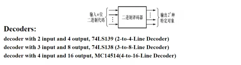
因为任意组合逻辑函数都可以写成 sum of minterms 的形式,我们可以用二进制译码器+或门来表示任意组合逻辑
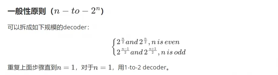
Decoders with Enable
在普通译码器的基础上多一个使能信号(enable) EN 来控制,当 EN 为 0 时无论 什么值都输出全零,否则输出对应的最小项。
Demultiplexers
cm:不考。
我们可以通过带使能信号的译码器,将来自一条输入线上的信息传送到 条输入线中的指定一条,实现分配(distribution) 功能。
实现这一功能的电路称为多路分配器(demultiplexer = demux)。一个带使能的 - 译码器又是一个 1- 多路分配器。其中 1 指的是输入信号的位宽(bit width) 是 1,这一输入直接接到 EN 输入处。
BCD-to-Seven-Segment Decoder
实现 7 位数码管译码器,可以通过逻辑门实现布尔函数,也可以直接用上面实现多路分配器。
关于 7 位数码管内部构造,可采用共阳极(common anode) 接法或共阴极(common cathode) 接法,其中前者是 0 触发,后者是 1 触发。参见下图:
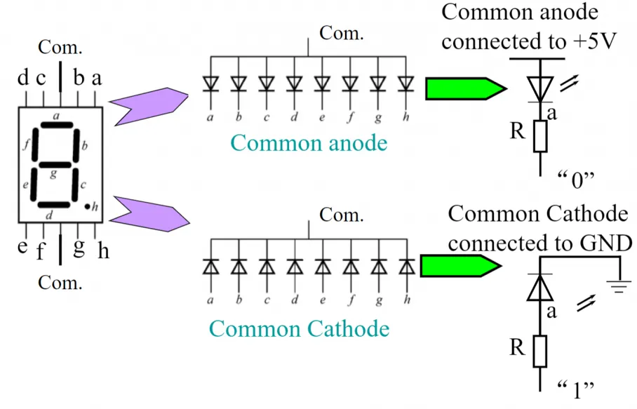
Encoders
编码(encoding):the conversion of an -bit input code to a -bit output code with such that each valid code word produces a unique output code.
Priority Encoders
优先编码器(priority encoder) 的作用是的当多个输入同时为 1 时,优先级最高的输入需要被优先处理。所以我们需要实现一个编码器,输出优先级最高的为 1 的输入是多少。其真值表如下:
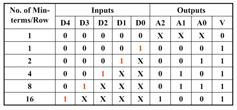
可以提供不少无关项用于化简。
别忘了怎么化简
e.g. 。
Multiplexers
用一组 位的输入信号(称为选择输入(selection input))选择 位的输入信号中的一路到输出,实现这一功能的电路称为多路选择器(multiplexer = mux),也被叫作多路分配器。
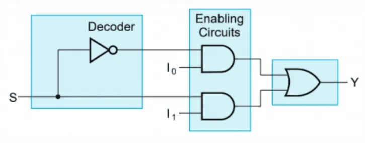
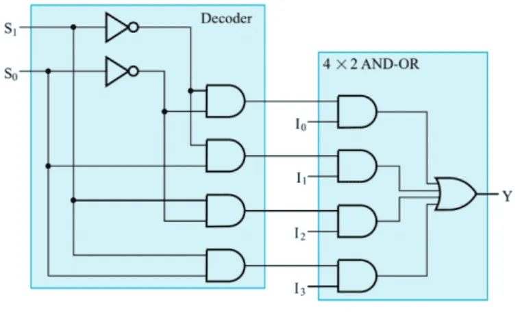
一般来说,一个 -to- line MUX 需要有 -to- line decoder 和 个 AND 以及一个 OR:
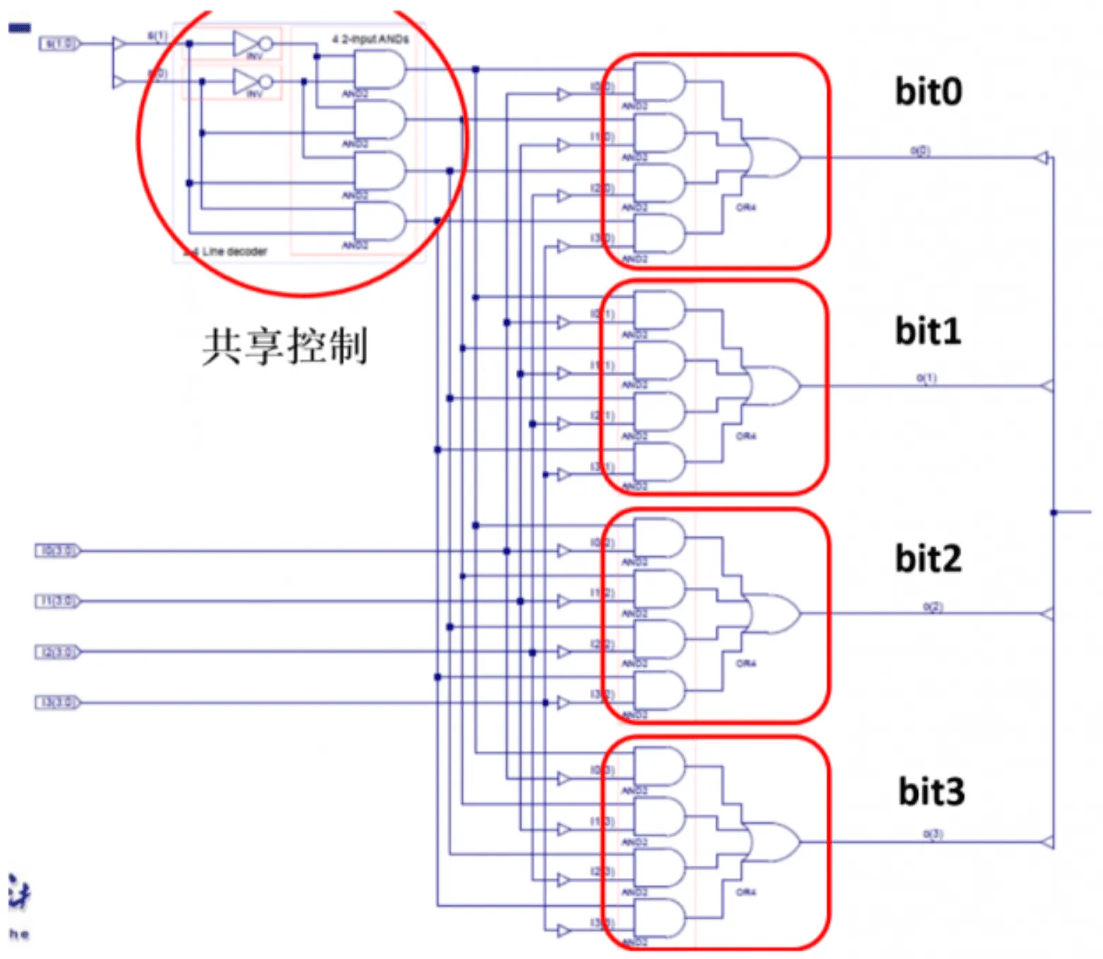
这里介绍的 MUX 还是 1bit 的,我们也可以一次性做多位,这样的话只需要一个选择模块。下面以 4bits 4-to-1 MUX 为例:
Binary Adders
Half Adders
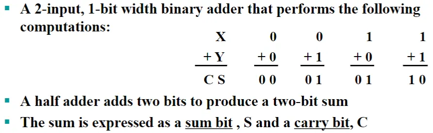
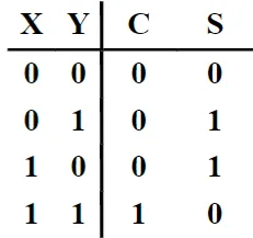
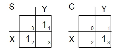
半加器(half-adder):实现两位相加的组合电路。
| 真值表 | 卡诺图 | 逻辑函数 |
|---|---|---|
 |  | 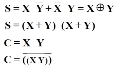 |
如果我们选用不同的逻辑函数,就可以有不同的电路实现。其中,最常见的半加器实现如下:
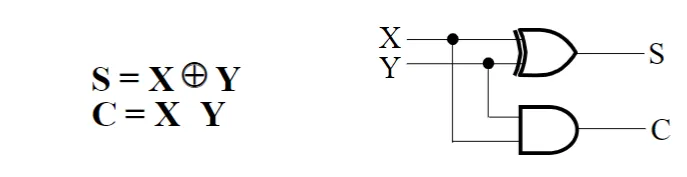
一个只使用 NAND 门的半加器实现如下:
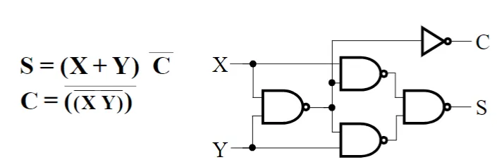
Full Adders
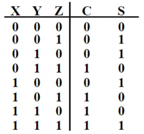
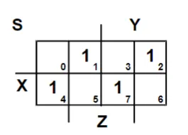
全加器(full-adder):实现三位相加(两位及一位进位(carry-in bit))的组合电路。
| 真值表 | 卡诺图 |
|---|---|
 |  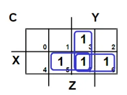 |
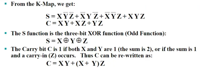
-
进位产生函数(carry generate function) - :当 和 都是 时就会发生进位。一般简写成 。
-
进位传递函数(carry propagate function) - :当 和 中恰有一个是 的话,如果收到一个来自低位的进位,就一定会传递给高位。一般简写成 。
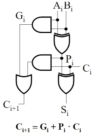
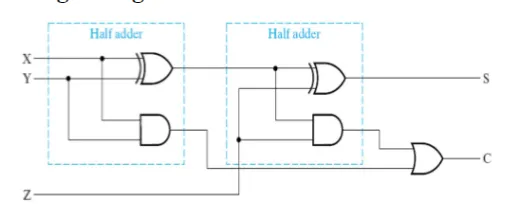
一个全加器相当于由两个半加器组成,因为实际上你就是把 三个数加起来,用了两个半加:
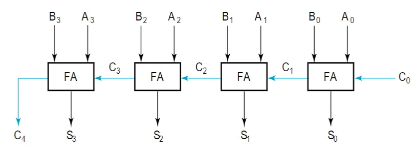
Ripple-Carry Adders
Carry-Lookahead Adders
这里仅做了解,在《计算机组成》课程中会进一步介绍。
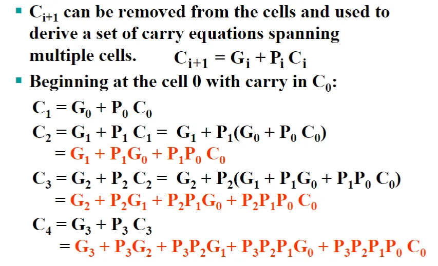
通过把进位展开,我们直接计算最后产生的进位,这里以 4bit 的超前进位加法器为例:
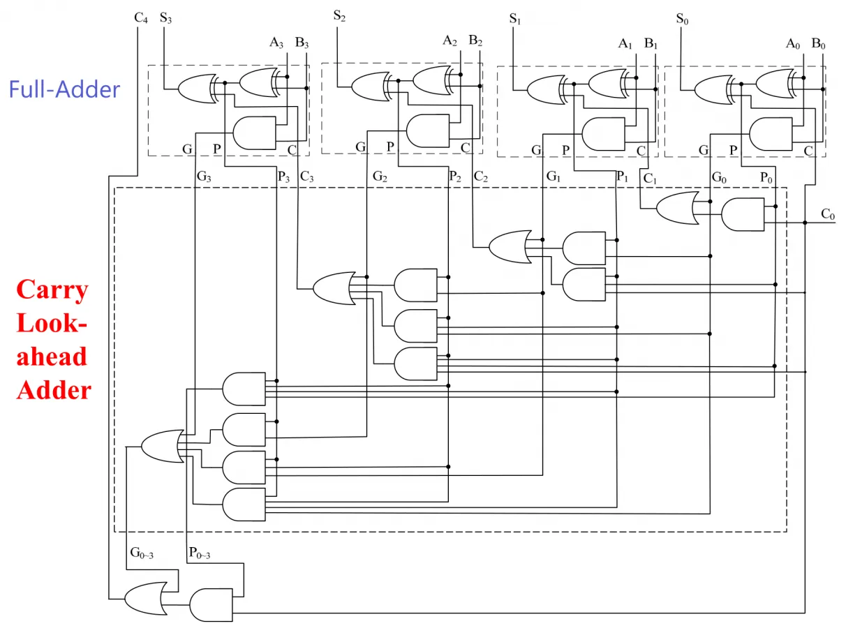
其电路实现如下:
考察超前进位加法器的性能:
- 全加器部分:从 变成 ,只需要经过一个异或门,消耗 3 单位时间。
- CLA 部分:虽然看起来有很多个 AND、看起来电路很复杂,但是注意到与门可以多输入同时做,故实际信号只经过了一个与门和一个或门,消耗 2 单位时间。
- 再回到全加器部分:像 信号,不像 可以直接输出,需要回到全加器部分再经过一个异或门,消耗 单位时间。
这样我们就得到了一个最大延迟只有 个单位的 4bit 超前进位加法器。
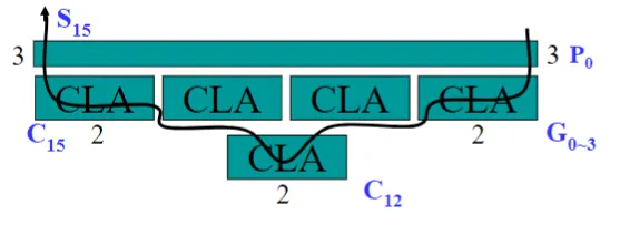
那如果我们需要 16-bit 的超前进位加法器呢?注意到中间门电路的输入数量是 级别的,如果一味增大 CLA,消耗的成本太高。实际上,只需要把上面电路图中的全加器替换成 CLA,就是一个 16 位的超前进位加法器。(4-bit:全加器 CLA;16-bit:全加器 CLA CLA)
计算此实现下的 16-bit 超前进位的性能:
Binary Subtractors
- 被减数(minuend)
- 减数(subtrahend)
反码(one’s complement)
可以通过二进制按位取反得到。
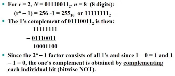
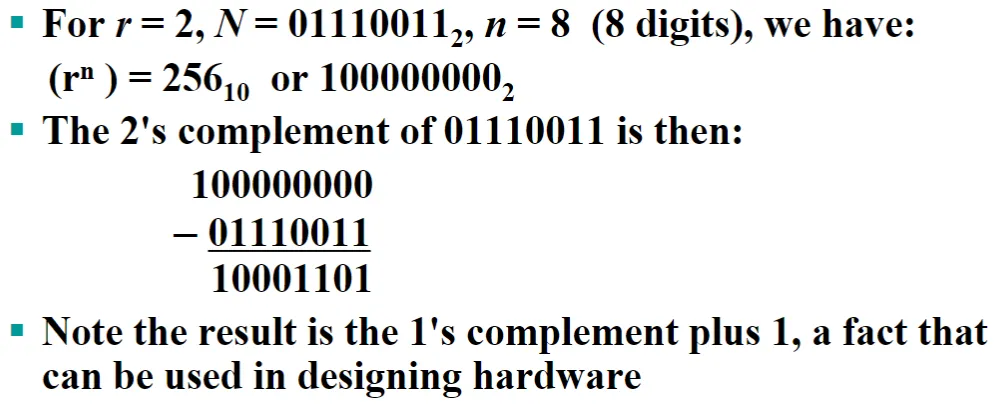
补码(two’s complement)
可以通过反码加 1 得到。一般来说,我们直接用补码来存储负数,相当于是一个硬件层面的约定。
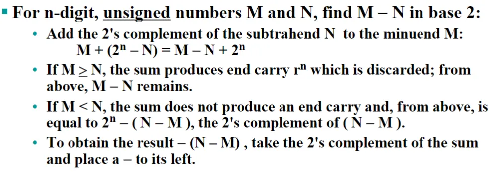
Unsigned Subtraction
方法如下:
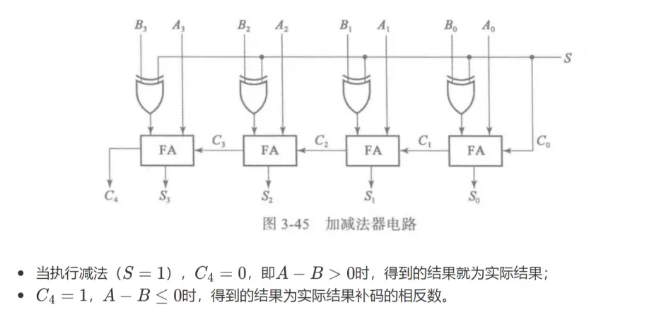
Clarification
这里无符号减法的说法其实比较迷糊,我们暂且不承认符号位(也就是用补码表示负数)这一事实。以 4-bit 为例,相当于处理两个 值域的数 的 。如果结果是负数(在值域外),就应得到负数取反的结果,然后再“手动”填上一个负号。即计算 时我们希望得到 和一个负号,而不是直接得到 ,这就是为什么上文 时需要多取一次补码。
Signed Subtraction
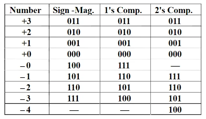
有符号整数(signed integer) 的表示方法
最高位都是符号位,然后:
- Signed-Magnitude:负数时,低 位表示其绝对值
- Signed 1’s Complement:负数时,低 位表示其绝对值的反码
- Signed 2’s Complement:负数时,低 位表示其绝对值的补码
使用前两种方法会出现 和 的两种表示。一般来说,前两种方法比大小时比较方便,第三种方法做加减法比较方便,这也是我们要介绍的。
Overflow Detection
在同符号数字相加、异符号数相减时可能发生溢出。
Comments